Technical Paper Title: MILLIPEDE – AN ULTRA DENSE DATA STORAGE TECHNOLOGY
Authors: Inturi Ramu, 2nd BTech, ECE
College: Prakasam Engineering College, Kandukur
ABSTRACT:
This paper focuses on the field of nano memory storage systems. It in particular discusses about a research project named “Millipede” under development at IBM labs.
In this, nanometer-sharp tips are used to scan the storage surface and to write and read data. In this, storage densities of up to 500 Gbit/in2 can be achieved by thermo mechanical writing and reading using probe tips. This concept combines ultrahigh density, gigabit capacity and high data rate. The concept of data storage using this technique and the principles of operation (write, read and erase) are dealt with elaborately in this paper. A practical read channel model and its mathematical analysis are also presented. The evolution of the Millipede is described and technical specifications are provided. Moreover applications, challenges faced by the system and its advantages are discussed. The experimental data, mathematical equations and general figures have been borrowed by the authors to prepare the paper on the topic
INTRODUCTION:
In today’s high tech world, information is denoted by 0’s and 1’s i.e. the binary language. This is widely used in computer and electronic devices. Thus, any system designed to store information must be able to represent 1’s and 0’s in a easy and legible manner. Various methodologies are used in different media to store these bits. The primary and most commonly used form of storage viz magnetic storage uses magnetic domains to store data.
Orientations of these domains represent the binary bits.Presently, the storage density is about 75 – 150 Gbits/in2 and densities about that are not feasible and stable due to super paramagnetic limit. So this form of storage is not able to keep up with the ever growing need for more storage and thus the necessity for hi density storage medium is inevitable.
The solution for this comes in the form of nanotechnology in which probe tips are used to store data on a nano scale thereby increasing exponentially the storage.
This is an emerging concept widely being researched for its possibilities. According to this concept, the surface of the storage medium is scanned by cantilever attached probe tips using the AFM and STM techniques. Indentations are made in the surface using the tips to represent the 1’s and no indentations represent the 0’s. In this device read, write and erase functions are possible which will be discussed elaborately later in the paper. Usually, data rates achieved by using a single probe tip are well below prevalent transfer rates and so arrays of cantilevers operating in parallel, with each cantilever performing read/write/erase operations over an individual storage field are generally used.
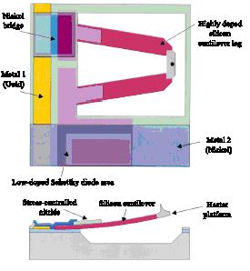
“Millipede” promises storage densities of upto 500 to 1000 Gbit/in.2 using a parallel operation of about (32×32) AFM cantilever arrays with integrated probe tips. The principle of Millipede is explained below and a prototype model is introduced later in the paper.
KEY TERMS:
Cantilever:
It is a silicon platform whose one end is fixed and a probe tip is attached to another end which is free to move in the vertical axis by the application of a mechanical force.
A F M (Atomic Force Microscope):
This is an instrument with a scanning tip which sends signals that depend on the magnitude of the atomic forces between particles on the surface and the tip. As the strength of these signals depend on the distance between the tip and the particle, they can be used to interpret the distribution of particles on the sample surface
S T M (Scanning Tunneling Microscope):
In this instrument a voltage is applied to the sharp tip which is very close to the surface of the sample. This voltage attracts electrons from the material of the surface resulting in weak current. As the current magnitude depends on the distance between the tip and the particle on the surface a three dimensional plot can be drawn which gives an idea about the sample surface.
Thermo mechanical sensor:
This senses the variations of temperature and sends electrical signals whose value depends on the magnitude of temperature differences.
Form factor:
This is defined as the area required to store 1Gbit of data. It is usually in the order of centimeters for a Millipede device.
Piezoresistive sensing:
This type of read mode was used in first generation Millipede devices. In this type of sensing, an applied electric signal bends the cantilever which moves into the pit (in case of 1) and mechanical strain is developed. Due to piezoelectric effect, an electric pulse is produced, which when sent to the resistor bridge, produces a voltage which is detected by a detection circuit.
PRINCIPLES OF OPERATION OF THE MILLIPEDE:
The Millipede device is a highly parallel scanning-probe data-storage system, where information is stored as sequences of .indentations and .no indentations written on nanometer-thick polymer films using an array of AFM cantilevers.
The Write Read and Erase operations of the Millipede device are as follows.
WRITE OPERATION:
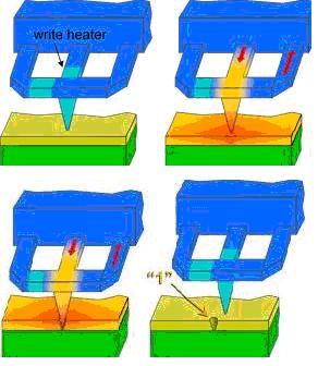
As explained earlier, information is stored in the form of 1’s and 0’s by making indentations and no indentations in the storage medium. This is achieved by a process called thermo mechanical writing which involves both mechanical and heating operations. In this process, the probe tip is heated using local heaters which soften the storage surface making it ready for writing. The heating makes it easier to penetrate the surface. Initially, the heating from the tip to the storage medium is through air which inhibits the heat transfer, but this improves as the contact area increases when the tip moves into the surface. This means that the tip must be heated to a relatively high temperature of about 400ºC to initiate the softening. Simultaneously, an electric pulse is sent to the cantilever which bends due to the atomic attraction between atoms on the medium surface and on the tip.
This bending presses the tip into the polymer, forming an indentation, which is denoted as 1.Once softening has initiated, wherever a binary 1 has to be written on the storage medium there the tip is pressed into the polymer, hence forming an indentation and on the other hand for a binary 0 to be written no indentation is made which clearly distinguishes 1’s and 0’s.Also, to form a stable indentation the local surface must be rapidly cooled after the write operation.
Thermo mechanical writing of data in this manner can make the storage medium to occupy bits of about 40nm size without being merged, implying a potential storage density on the order of 400 Gbit/in.2.
For example, a (32×32) cantilever array with 1024 storage fields, each having an area of 100×100 m2, has a capacity of about 6 G bit on a chip area on the order of 3×3 mm2. More recently single-cantilever areal densities up to 1 Tbit/in2 have been demonstrated, although currently at a somewhat degraded write/read quality.
READ OPERATION:
Information stored in the form of indentations and non-indentations on the surface can be read only when there is a conspicuous way of distinguishing them. The reading operation should involve a convenient process identifying them and designate 0’s and 1’s accordingly. To achieve this, the same probe tip attached cantilever is used. Also, the temperature dependent resistance of the probe tip is the main principle behind the read operation.
In general, the resistance increases nonlinearly with heating power/temperature from room temperature to a peak value of 500-700ºC. The peak temperature is determined by the doping concentration of the heater platform, which ranges from 1×10¹⁷ to 2×1018 cm.3. First the tip is heated to a temperature of about 350oC so that the storage surface does not melt. Then the cantilever is bent by applying a read electrical pulse which in turn produces a mechanical force. As the tip moves into the indentation the heat transfer rate improves and so the cantilever cools. This temperature decrease produces a change in resistance of about 10-4 to 5×10⁻⁴. This change in resistance is converted by a thermo mechanical sensor into an electrical signal. This sensor can be approximated to a variable resistance and the voltage across this resistance is detected by the detector, which produces a binary 1. The change in electrical resistance of the cantilever during this process is of the same order .Thus, a signal of high resolution is required to distinguish between these two changes in resistance and to read the information correctly.
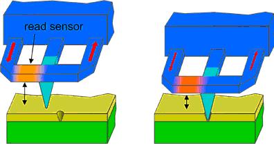
The maximum temperature attained by the cantilever while moving over an indentation is always less than the temperature attained when there is no indentation present. As the value of the variable resistance depends on the temperature of the cantilever, the maximum value achieved by the resistance will be smaller as the cantilever moves over an indentation. Therefore, during the read process, binary 1’s and 0’s can be easily distinguished and transmitted.
ERASE OPERATION:
In the thermal-mechanical writing process described above, indentations are created by applying a force on the cantilever.
Then the indent surface is rapidly cooled, resulting in the creation of a “meta-stable” indentation.
If the storage medium is reheated, it softens, thereby allowing relaxation of the surface and hence erasing the indentation. This can be done at the individual bit level by using the tip as a localized heat source.
Also, another way of erasing the old indentation is to write the new indentation very close to the old one thus erasing it. Hence, a previously written data track can be erased simply by overwriting it with a series of closely spaced indentations. In other words, erasing is essentially similar to writing at a narrower pitch between indentations.
READ CHANNEL MODEL:
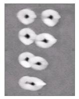
In this section, we consider the read back channel for a single cantilever, scanning a storage field where bits are written as indentations or no indentations. The circuit diagram used as read channel model, which we consider for the analysis of the detection system, is illustrated in Fig1. As discussed earlier, a cantilever can be considered as a variable resistance that depends on the temperature at the cantilever tip. To evaluate the evolution of the temperature of a heated cantilever during the read process, we use a simple RC-equivalent thermal circuit, as illustrated in Fig 2 where denote the thermal resistance and capacitance, respectively. The parameter indicates the relative variation of thermal resistance resulting from the small change in the air gap width between the cantilever tip and the storage medium when an indentation is present, as compared to the case with no indentations. Here subscript x indicates the x-distance in the direction of scanning from the initial point. Therefore, the parameter x will assume the largest absolute value when the tip of the cantilever is located at the center of an indentation. The heating power that is dissipated in the cantilever heater region is expressed as

where VC(t) is the voltage across the cantilever, T (t,x)
is the cantilever temperature, and Re(T (t,x))is the temperature-dependent cantilever resistance.
Figure1: Block diagram of the detection circuit.
As the heat-transfer process depends on the value of the thermal resistance and on the read-pulse waveform, temperature T(x, t) depends on time t and distance x. However, as the time it takes for the cantilever to move from the center of a logical mark to the next is much larger than the duration of a read pulse, we assume that T(x,t) does not vary significantly as a function of x during the period a read pulse is applied, and that it decays to the ambient temperature To before the next pulse is applied. Therefore the evolution of the cantilever temperature in response to a pulse applied at time t=xo/v, at a certain distance xo from the initial point of scanning and for a certain constant velocity v of the scanner, obeys a first order ,first degree differential equation involving T w.r.t to time ‘t’ say, eqn.(2) given below
T’ (t, x0) + [(T (t,x0)-T0)/ (RT(1+η xo)CT) ] = V2 C(t) /[( CTRe(T(t,x0)]
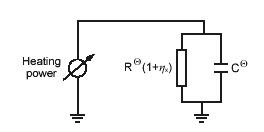
Figure 2: RC – equivalent thermal model of the heat transfer process.
With reference to the block diagram of the read channel illustrated in Fig .the source generates the read pulse that is applied to the cantilever variable resistance. Furthermore, the active low-pass RC detector filter used to eliminate high frequency noise, where Rlpf and Clpf denote the resistance and capacitance of the low-pass filter, respectively, is realized using an ideal operational amplifier that exhibits infinite input impedance, zero output impedance, and infinite frequency-independent gain. The read back signal Vo (t,xo) which is obtained at the low-pass filter output in response to the applied voltage Vp(t) where,
Vp (t) = Arect ((t-t0)) and
rect (t/ τ) = 1 for 0≤t≤ τ
0 elsewhere
Vp (t) obeys a complex differential equation, say equation (3) presented here.
V0’ (t, x0)
=(Rlpf Clpf)-1 [ -Vo(t,x0)+ [ Rlpf x Vp (t)]/(Re(T(t,x0)) ]
As the voltage at the output of the low-pass filter depends on the variable resistance value the read back signal is determined by solving jointly the differential equations Vo(to,x),with initial conditions T(xo,to)=To, Vo (to,xo)=0 the duration of the applied rectangular pulse. Assuming that ideal control of the scanner is performed, such that the time of application of a read pulse corresponds either to the cantilever being located at the center of an indentation for detecting a bit .1., or away from an indentation for detecting a bit .0., two possible responses are obtained at the output of the low- pass filter as solutions of (2) and (4), which we denote by Vo (ts, xo|αxo=1)-Vo (ts, xo|αxo=0) respectively. By sampling the read back signal at the instant, ts=to+τ
Simple threshold detection may be applied to detect a bit.
The threshold voltage is given by:
VTh=1/2[Vo (ts, xo|αxo=1) +Vo (ts, xo|αxo=0)]
The read back signal (6) at the output of the low-pass filter is observed in the presence of additive noise. Therefore, the read back signal for detection of the i-th binary symbol is given by
r (ts, i) =s (t s, i) +w (t s, i)
where w (t) denotes the noise signal. The components of the noise signal that must be taken into account are thermal noise from the sensor and the reference cantilever resistances, which during the read process achieve a temperature of about 350ºC, and from the low-pass filter resistance, as well as noise from equivalent noise sources in the operational amplifier.
To determine system performance, we evaluate the signal-to-noise ratio at the detection point, expressed as
SNR = 10log10 (V2th1/σ2w)
Where, Vth1 is the threshold voltage at detection and is σ2w the variance of noise.
CONTROL MODEL:
Write/read operations depend on a mechanical parallel x/y scanning of either the entire cantilever array chip or the storage medium. The tip-medium contact is maintained and controlled as a whole, i.e., not on an individual cantilever basis, by using a common control for the entire chip, which greatly simplifies the system.
Experimental results indicate that overall chip tip-apex height control to within 500 nm is feasible.
As the Millipede tracks the entire array without individual cantilever positioning, thermal expansion of the array chip has to be small. For 3×3 mm2 silicon array area and 10-nm tip-position accuracy, the chip temperature has to be controlled to about 1ºC. This is ensured by four temperature sensors in the corner of the array and heater elements on each side of the array. Thermal-expansion is the reason why two-dimensional arrays are preferred over one dimensional ones which would utilise space on the storage medium more efficiently
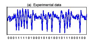
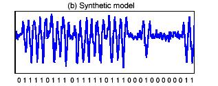
Figure 3: Comparison between (a) the read back signal obtained experimentally along a data track and (b) the read back signal obtained by the synthetic model.
FIRST GENERATION MILLIPEDE:
As a first step, a (5 x5) array chip was designed and
fabricated to test the basic Millipede concept. All 25 cantilevers had integrated tip heating for thermo mechanical writing and piezoresistive deflection sensing for read-back. Each cantilever was individually addressable for both thermo mechanical writing and piezoresistive deflection sensing. A complete resistive bridge for integrated detection has also been incorporated for each cantilever. Unfortunately, the chip was not able to demonstrate parallel writing because of electro migration problems due to temperature and current density in the Al wiring of the heater.
Once global leveling was proven as a reliable concept and (Al) wiring was avoided, the millipede was a realizable device. Using the results of the (5×5) cantilever array, a (32×32) array chip was made with some important changes in the chip functionality and fabrication processes. The major differences are:
1) Surface micromachining to form cantilevers at the wafer surface,
2) All-silicon cantilevers,
3) Thermal instead of piezoresistive sensing,
4) First- and second-level wiring with an insulating layer for a multiplexed row/column addressing scheme.
Since the heater platform was both a write/read element and no individual cantilever actuation was required, the basic array cantilever cell became a simple device.
TECHNICAL SPECIFICATIONS:
The present day specifications for a (32×32) Millipede device are.
1. The cell area and x/y cantilever pitch is 92 µm x 92 µm, which results in a total array size of less than 3 mm x 3 mm for the 1024 cantilevers.
2. The cantilever is fabricated entirely of silicon for good thermal and mechanical stability. It consists of the heater platform with the tip on top, the legs acting as a soft mechanical spring, and an electrical connection to the heater. They are highly doped to minimize interconnection resistance and replace the metal wiring on the cantilever to eliminate electro migration.
3. The resistive ratio between the heater and the silicon interconnection sections should be as high as possible; currently the highly doped interconnections are 400 Ω and the heater platform is 11 k Ω (at 4 V reading bias).
4. The cantilever must be soft (low mass) to avoid high loading forces and to achieve high resonant frequencies. This leads to less wear and tear and higher speed of operation.
5. Keeping the above considerations in mind, the array cantilever is designed to be 50-µm-long, 10-µm-wide, 0.5-µm-thick at the legs, and 5-µm-wide, 10-µmlong, 0.5-µm-thick at the platform platform. This cantilever has a stiffness of 1 N/m and a resonant frequency of 200 kHz.
6. The heater time constant is a few microseconds, which
should allow a multiplexing rate of 100 kHz.
7. A large gap is required between the tip and the medium, but the tips must be sort to improve sensitivity, we purposely bent the cantilevers a few micrometers out of the chip plane by depositing a silicon nitride layer at the base of the cantilever.
8. The cantilevers within the array are electrically isolated from one another by integrated Schottky diodes. Because every parasitic path in the array to the addressed cantilever of interest contains a reverse-biased diode, the crosstalk current is drastically reduced.
9. The tip-apex height uniformity within an array is to be maintained because it determines the force of each
cantilever while in contact with the medium and hence
influences write/read performance as well as medium and tip wear.
STRENGTHS:
1. Very high storage density of about 500Gbit/in2 is possible.
2. High data rates are achieved through massive parallelism.
3. Control loop structure for optimized 2D motion has been established.
4. Track following with nm precision is achieved.
5. It consumes very low power compared to other devices.
6. It has reliable operation with small overhead.
CHALLENGES:
1. The medium must endure long term usage.
2. It must endure long term tip & media wear.
3. Tip uniformity in lever array chip must be maintained.
4. It must be shock resistant and immune to vibrations.
5. Cantilever must be designed for low power reading & writing/
6. The area density limits must be exploited to the maximum permissible safe limit.
7. The signals must be processed and detected accurately for proper operation.
APPLICATIONS:
There are many applications for the Millipede chip in storage devices. The concept and design vary according to the required application. Two cases in particular are discussed below.
Terabit drive:
The potential for very high storage density makes the
Millipede very attractive for high-end terabit storage
applications also. Terabit capacity can be achieved in three methods:
1) Very large arrays,
2) Many smaller arrays operating in parallel and
3) Displacement of small/medium-sized arrays over large disk.
Though realization of considerably larger arrays
(105 to 106 cantilevers) appears to be possible, control of
the thermal linear expansion will be a delimiting factor as the array chip becomes significantly larger and control problems will definitely arise.
The second approach is appealing because the storage system can be upgraded to fulfill our requirements in a modular fashion by operating many smaller Millipede units in parallel.
The operation of the third approach is described with the example of a modified hard disk. This approach has the advantage of integration of new technology with our existing systems. A number of small arrays on the disk which can be accessed in a way similar to that of the present hard drive enhance the storage capacity greatly while keeping the basic principle unchanged. A storage capacity of several terabits appears to be achievable on 2.5- and 3.5-in. disks.
Nanodrive:
Using the concept of Millipede, storage devices with gigabyte capacity having a very small form factor in the range of centimeters and even millimeters can be made possible. Hence this concept opens up possibilities to integrate such “Nanodrives” into low power consuming devices such as watches, cellular telephones, laptops, etc.
Millipede based nanodrives have interesting prospects for audio and video consumer applications. All-silicon, batch fabrication, low-cost polymer media, and low power consumption make Millipede very attractive as a centimeter- or even millimeter-sized gigabyte storage system.
CONCLUSION:
The field of nano storage is an upcoming field with new discoveries being made everyday. This form of storage for example, Millipede has an unprecedented storage density and the possibilities it opens up are limitless.
Also, the other advantages possessed the system like speed of access and low power consumption make it an ideal choice to fulfill the burgeoning memory demand. Its small dimensions are an additional advantage as it can be used in portable and mini systems. This technology is in development but further research can only reveal better features which will be incremental towards commercial success.
Thus, if the system is promoted properly and developed correctly, it will be the way of the feature for storage systems.
REFERENCES:
1. Understand Electronics by O N Bishop – 2001
2. P. Vettiger, M. Despont, U. Drechsler, U. Dürig, W. Häberle, M. I. Lutwyche, H. E. Rothuizen, R. Stutz, R. Widmer, and G. K. Binnig, .The. Millipede. – More than One Thousand Tips for Future AFM
Data Storage, IBM J. Res. Develop., 44 (2000),
3. P. Vettiger, G. Cross, M. Despont, U. Drechsler, U. Dürig, B. Gotsmann, W. Häberle, M. A. Lantz, H. E. Rothuizen, R. Stutz and G. K. Binnig, The .Millipede. Nanotechnology Entering Data Storage, IEEE Trans. Nanotechnology. vol. 1, no. 1 (2002, in press).
4. G. Binnig, H. Rohrer, Ch. Gerber and E. Weibel, 7×7 Reconstruction on Si (111) Resolved in Real Space, Phys. Rev. Lett., 50 (1983) pp. 120-123.
5. Nanometer Scale Science and Technology by M. Allegrini


