Technical Paper Title: Solar and fuel cell technology
Authors:A.Sai Pavani, T.Tejovathi & K.S.N.Avanthi, 2nd year BTech,EEE
College: Sai Spurthi Institute Of Technology, Sattupally, Khammam
Abstract
A solar cell is a device that converts the energy of sunlight directly into electricity by the photovoltaic effect. Sometimes the term solar cell is reserved for devices intended specifically to capture energy from sunlight such as solar panels and solar cells, while the term photovoltaic cell is used when the light source is unspecified. Assemblies of cells are used to make solar panels, solar modules, or photovoltaic arrays. Photovoltaics are the field of technology and research related to the application of solar cells in producing electricity for practical use. The energy generated this way is an example of solar energy (also known as solar power)
PHOTOVOLTAIC EFFECT
The photovoltaic effect involves the creation of a voltage (or a corresponding electric current) in a material upon exposure to electro-magnetic radiation. Though the photovoltaic effect is directly related to the photoelectric effect, the two processes are different and should be distinguished.In the photoelectric effect electrons are ejected from a material’s surface upon exposure to radiation of sufficient energy. The photovoltaic effect is different in that the generated electrons are transferred from different bands (i.e. from the valence to conduction bands) within the material, resulting in the buildup of a voltage between two electrodes.
In most photovoltaic applications the radiation is sunlight and for this reason the devices making use of the photovoltaic effect to convert solar energy into electrical energy are known as solar cells. In the case of a p-n junction solar cell, illumination of the material results in the creation of an electric current as excited electrons and the remaining holes are swept in different directions by the built-in electric field of the depletion region
INTRODUCTION
1. Photons in sunlight hit the solar panel and are absorbed by semiconducting materials, such as silicon.
2. Electrons (negatively charged) are knocked loose from their atoms, allowing them to flow through the material to produce electricity. Due to the special composition of solar cells, the electrons are only allowed to move in a single direction.
3. An array of solar cells converts solar energy into a usable amount of direct current (DC) electricity
CONTENTS:
• HISTORY OF SOLAR CELL
• HIGH EFFICIENCY CELL
a)RECORD EFFICIENCICES
• TYPES OF SOLAR CELLS
• A)MULTIPLE-JUNCTION SOLAR CELLS
• B)THIN-FILN SOLAR CELLS
• C)CRYSTALLINE SILICON
• THEORY OF SOLAR CELLS
• EQUIVALENT CIRCUIT
• SILICON SOLAR CELL DEVICE NANUFACTURE
• LIGHT ABSORBING MATERIALS
• APPILICATION AND IMPLEMENTATION
• CONCLUSION
HISTORY OF SOLAR CELL:
The term “photovoltaic” comes from the Greek (phōs) meaning “light”, and “voltaic”, meaning electric, from the name of the Italian physicist Volta, after whom a unit of electro-motive force, the volt, is named. The term “photo-voltaic” has been in use in English since 1849.The photovoltaic effect was first recognized in 1839 by French physicist A. E. Becquerel. However, it was not until 1883 that the first solar cell was built, by Charles Fritts, who coated the semiconductor selenium with an extremely thin layer of gold to form the junctions. The device was only around 1% efficient. Subsequently Russian physicist Aleksandr Stoletov built the first solar cell based on the outer photoelectric effect (discovered by Heinrich Hertz earlier in 1887). Albert Einstein explained the photoelectric effect in 1905 for which he received the Nobel prize in Physics in 1921. Russell Ohl patented the modern junction semiconductor solar cell in 1946which was discovered while working on the series of advances that would lead to the transistor
HIGH EFFICIENCY CELLS
High-efficiency cells
High-efficiency solar cells are a class of solar cell that can generate more electricity per incident solar power unit (watt/watt). Much of the industry is focused on the most cost efficient technologies in terms of cost per generated power. The two main strategies to bring down the cost of photovoltaic electricity are increasing the efficiency of the cells and decreasing their cost per unit area. However, increasing the efficiency of a solar cell without decreasing the total cost per kilowatt-hour is not more economical, since sunlight is free. Thus, whether or not “efficiency” matters depends on whether “cost” is defined as cost per unit of sunlight falling on the cell, per unit area, per unit weight of the cell, or per unit energy produced by the cell. In situations where much of the cost of a solar system scales with its area (so that one is effectively “paying” for sunlight), the challenge of increasing the photovoltaic efficiency is thus of great interest, both from the academic and economic points of view. Many groups have published papers claiming possibility of high efficiencies after conducting optical measurements under many hypothetical conditions. The efficiency should be measured under real conditions and the basic parameters that need to be evaluated are the short circuit current, open circuit voltage
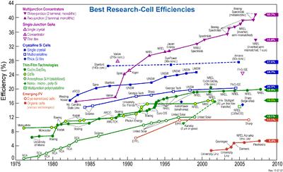
The chart at the right illustrates the best laboratory efficiencies obtained for various materials and technologies, generally this is done on very small, i.e. one square cm, cells. Commercial efficiencies are significantly lower.
RECORD EFFICIENCES
A March 2010 experimental demonstration of a design by a Caltech group may be more efficient still; it has an absorption efficiency of 85% in sunlight and 95% at certain wavelengths (it is claimed to have near perfect quantum efficiency).[31] However, absorption efficiency should not be confused with the sunlight-to-electricity conversion efficiency.
TYPES OF SOLAR CELLS
Multiple-junction solar cells
The record for multiple junction solar cells is disputed. Teams led by the University of Delaware, the Fraunhofer Institute for Solar Energy Systems, and NREL all claim the world record title at 42.8, 41.1, and 40.8%, respectively. ectrolab also claims commercial availability of cells at nearly 42% efficiency in a triple junction design; the cost is breathtaking. NREL claims that the other implementations have not been put under standardized tests and, in the case of the University of Delaware project, represents only hypothetical efficiencies of a panel that has not been fully assembled NREL claims it is one of only three laboratories in the world capable of conducting valid tests, although the Fraunhofer Institute is among those three facilities.
A March 2010 experimental demonstration of a design by a Caltech group may be more efficient still; it has an absorption efficiency of 85% in sunlight and 95% at certain wavelengths (it is claimed to have near perfect quantum efficiency).[31] However, absorption efficiency should not be confused with the sunlight-to-electricity conversion efficiency.
Thin-film solar cells
In 2002, the highest reported efficiency for thin film solar cells based on CdTe is 18%, which was achieved by research at Sheffield Hallam University, although this has not been confirmed by an external test laboratory.
The US national renewable energy research facility NREL achieved an efficiency of 19.9% for the solar cells based on copper indium gallium selenide thin films, also known as CIGS (also see CIGS solar cells).
NREL has since developed a robot that builds and analyzes the efficiency of thin-film solar cells with the goal of increasing the efficiency by testing the cells in different situations.
These CIGS films have been grown by physical vapour deposition in a three-stage co-evaporation process. In this process In, Ga and Se are evaporated in the first step; in the second step it is followed by Cu and Se co-evaporation and in the last step terminated by In, Ga and Se evaporation again.
Thin film solar has approximately 15% marketshare; the other 85% is crystalline silicon Most of the commercial production of thin film solar is CdTe with an efficiency of 11%.
Crystalline Silicon
The highest efficiencies on silicon have been achieved on monocrystalline cells. The highest commercial efficiency (22%) is produced by SunPower, which uses expensive, high-quality silicon wafers. The University of New South Wales has achieved 25% efficiency on monocrystalline silicon in the lab, technology that has been commercialized through its partnership with Suntech Power. Crystalline silicon devices are approaching the theoretical limiting efficiency of 29%and achieve an energy payback period of 1-2 years.
THEORY OF SOLAR CELLS
Photo generation of charge carriers
When a photon hits a piece of silicon, one of three things can happen:
1. the photon can pass straight through the silicon — this (generally) happens for lower energy photons,
2. the photon can reflect off the surface,
3. the photon can be absorbed by the silicon, if the photon energy is higher than the silicon band gap value. This generates an electron-hole pair and sometimes heat, depending on the band structure.
When a photon is absorbed, its energy is given to an electron in the crystal lattice. Usually this electron is in the valence band, and is tightly bound in covalent bonds between neighboring atoms, and hence unable to move far. The energy given to it by the photon “excites” it into the conduction band, where it is free to move around within the semiconductor. The covalent bond that the electron was previously a part of now has one fewer electron — this is known as a hole. The presence of a missing covalent bond allows the bonded electrons of neighboring atoms to move into the “hole,” leaving another hole behind, and in this way a hole can move through the lattice. Thus, it can be said that photons absorbed in the semiconductor create mobile electron-hole pairs.
A photon need only have greater energy than that of the band gap in order to excite an electron from the valence band into the conduction band. However, the solar frequency spectrum approximates a black body spectrum at ~6000 K, and as such, much of the solar radiation reaching the Earth is composed of photons with energies greater than the band gap of silicon. These higher energy photons will be absorbed by the solar cell, but the difference in energy between these photons and the silicon band gap is converted into heat (via lattice vibrations — called photonsrather than into usable electrical energy.
Charge carrier separation
There are two main modes for charge carrier separation in a solar cell:
1. drift of carriers, driven by an electrostatic field established across the device
2. diffusion of carriers from zones of high carrier concentration to zones of low carrier concentration (following a gradient of electrochemical potential).
The p-n junction
Main articles: semiconductor and p-n junction
The most commonly known solar cell is configured as a large-area p-n junction made from silicon. As a simplification, one can imagine bringing a layer of n-type silicon into direct contact with a layer of p-type silicon. In practice, p-n junctions of silicon solar cells are not made in this way, but rather by diffusing an n-type dopant into one side of a p-type wafer (or vice versa).
If a piece of p-type silicon is placed in intimate contact with a piece of n-type silicon, then a diffusion of electrons occurs from the region of high electron concentration (the n-type side of the junction) into the region of low electron concentration (p-type side of the junction). When the electrons diffuse across the p-n junction, they recombine with holes on the p-type side. The diffusion of carriers does not happen indefinitely, however, because charges build up on either side of the junction and create an electric field. The electric field creates a diode that promotes charge flow, known as drift current, that opposes and eventually balances out the diffusion of electron and holes. This region where electrons and holes have diffused across the junction is called the depletion layerbecause it no longer contains any mobile charge carriers. It is also known as the space charge region.
Connection to an external load
Ohmic metal-semiconductor contacts are made to both the n-type and p-type sides of the solar cell, and the electrodes connected to an external load. Electrons that are created on the n-type side, or have been “collected” by the junction and swept onto the n-type side, may travel through the wire, power the load, and continue through the wire until they reach the p-type semiconductor-metal contact. Here, they recombine with a hole that was either created as an electron-hole pair on the p-type side of the solar cell, or a hole that was swept across the junction from the n-type side after being created there.
Equivalent circuit of a solar cell
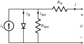
The equivalent circuit of a solar cell
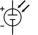
The schematic symbol of a solar cell
To understand the electronic behavior of a solar cell, it is useful to create a model which is electrically equivalent, and is based on discrete electrical components whose behavior is well known. An ideal solar cell may be modelled by a current source in parallel with a diode; in practice no solar cell is ideal, so a shunt resistance and a series resistance component are added to the model. The resulting equivalent circuit of a solar cell is shown on the left. Also shown, on the right, is the schematic representation of a solar cell for use in circuit diagrams.
SILICON SOLAR CELL DEVICE MANUFACTURE
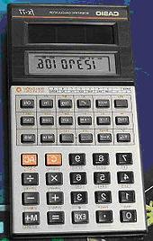
Solar-powered scientific calculator
Because solar cells are semiconductor devices, they share many of the same processing and manufacturing techniques as other semiconductor devices such as computer and memorychips. However, the stringent requirements for cleanliness and quality control of semiconductor fabrication are a little more relaxed for solar cells. Most large-scale commercial solar cell factories today make screen printed poly-crystalline silicon solar cells. Single crystalline wafers which are used in the semiconductor industry can be made into excellent high efficiency solar cells, but they are generally considered to be too expensive for large-scale mass production.
Poly-crystalline silicon wafers are made by wire-sawing block-cast silicon ingots into very thin (180 to 350 micrometer) slices or wafers. The wafers are usually lightly p-type doped. To make a solar cell from the wafer, a surface diffusion of n-type dopants is performed on the front side of the wafer. This forms a p-n junction a few hundred nanometers below the surface.
Antireflection coatings, which increase the amount of light coupled into the solar cell, are typically next applied. Over the past decade, silicon nitride has gradually replaced titanium dioxide as the antireflection coating of choice because of its excellent surface passivation qualities (i.e., it prevents carrier recombination at the surface of the solar cell). It is typically applied in a layer several hundred nanometers thick using plasma-enhanced chemical vapor deposition (PECVD). Some solar cells have textured front surfaces that, like antireflection coatings, serve to increase the amount of light coupled into the cell. Such surfaces can usually only be formed on single-crystal silicon, though in recent years methods of forming them on multicrystalline silicon have been developed.
The wafer then has a full area metal contact made on the back surface, and a grid-like metal contact made up of fine “fingers” and larger “busbars” are screen-printed onto the front surface using a silver paste. The rear contact is also formed by screen-printing a metal paste, typically aluminium. Usually this contact covers the entire rear side of the cell, though in some cell designs it is printed in a grid pattern. The paste is then fired at several hundred degrees Celsius to form metal electrodes in ohmic contact with the silicon. Some companies use an additional electro-plating step to increase the cell efficiency. After the metal contacts are made, the solar cells are interconnected in series (and/or parallel) by flat wires or metal ribbons, and assembled into modules or “solar panels”.
Light-absorbing materials
Main article: Absorption (electromagnetic radiation)
All solar cells require a light absorbing material contained within the cell structure to absorb photons and generate electrons via the photovoltaic effect. The materials used in solar cells tend to have the property of preferentially absorbing the wavelengths of solar light that reach the Earth surface. However, some solar cells are optimized for light absorption beyond Earth’s atmosphere as well. Light absorbing materials can often be used in multiple physical configurations to take advantage of different light absorption and charge separation mechanisms.
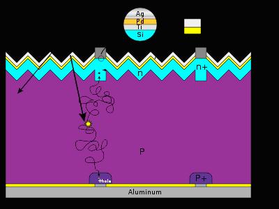
Crystalline silicon
Main articles: Crystalline silicon, Silicon, and list of silicon producers
Basic structure of a silicon based solar cell and its working mechanism.
By far, the most prevalent bulk material for solar cells is crystalline silicon (abbreviated as a group as c-Si), also known as “solar grade silicon”. Bulk silicon is separated into multiple categories according to crystallinity and crystal size in the resulting ingot, ribbon, or wafer.
1. monocrystalline silicon (c-Si): often made using the Czochralski process. Single-crystal wafer cells tend to be expensive, and because they are cut from cylindrical ingots, do not completely cover a square solar cell module without a substantial waste of refined silicon. Hence most c-Si panels have uncovered gaps at the four corners of the cells.
2. Poly- or multicrystalline silicon (poly-Si or mc-Si): made from cast square ingots — large blocks of molten silicon carefully cooled and solidified. Poly-Si cells are less expensive to produce than single crystal silicon cells, but are less efficient. US DOE data shows that there were a higher number of multicrystalline sales than monocrystalline silicon sales.
3. Ribbon sili is a type of multicrystalline silicon: it is formed by drawing flat thin films from molten silicon and results in a multicrystalline structure. These cells have lower efficiencies than poly-Si, but save on production costs due to a great reduction in silicon waste, as this approach does not require sawing from ingots.
Applications and implementations
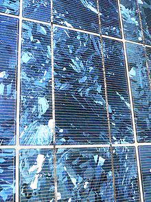
Polycrystaline photovoltaic cells laminated to backing material in a module
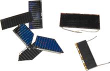
Polycrystalline photovoltaic cells
Main article: photovoltaic array
Solar cells are often electrically connected and encapsulated as a module. Photovoltaic modules often have a sheet of glass on the front (sun up) side, allowing light to pass while protecting the semiconductor wafers from the elements (rain, hail, etc.). Solar cells are also usually connected in series in modules, creating an additive voltage. Connecting cells in parallel will yield a higher current. Modules are then interconnected, in series or parallel, or both, to create an array with the desired peak DC voltage and current.
1. The power output of a solar array is measured in watts or kilowatts. In order to calculate the typical energy needs of the application, a measurement in watt-hours, kilowatt-hours or kilowatt-hours per day is often used. A common rule of thumb is that average power is equal to 20% of peak power, so that each peak kilowatt of solar array output power corresponds to energy production of 4.8 kWh per day (24 hours x 1 kW x 20% = 4.8 kWh)
To make practical use of the solar-generated energy, the electricity is most often fed into the electricity grid using inverters (grid-connected photovoltaic systems); in stand-alone systems, batteries are used to store the energy that is not needed immediately.
Solar cells can also be applied to other electronics devices to make it self-power sustainable in the sun. There are solar cell phone chargers, solar bike light and solar camping lanterns that people can adopt for daily use.
References
• ^ “NREL, DARPA Both Claim Record Solar Efficiency”. http://www.greentechmedia.com/articles/nrel-darpa-both-claim-record-solar-efficiency-1310.html. (A better citation would be preferred here. You can help Wikipedia by providing one.)
• ^ “Solar Spectral Irradiance: Air Mass 1.5”. National Renewable Energy Laboratory. http://rredc.nrel.gov/solar/spectra/am1.5/. Retrieved 2007-12-12.

